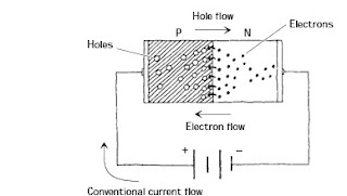
. Both n-type and p-type silicon conducts electric current; one does it with electrons (n-type), and the other does it with holes (p-type). Now the important feature to note here, which makes a diode work (act as a one-way gate) is the manner in which the two types of charge carriers interact with each other and how they interact with an applied electrical field supplied by an external voltage across its leads. Below is an explanation describing how the charge carriers interact with each other and with the electrical field to create an electrically controlled one-way gate.
Forward- bias(open door)
 when a diode is connected to a battery, as shown here, electrons from the n side and holes from the p side are forced toward the center (pn interface) by the electrical field supplied by the battery. The electrons and holes combine, and current passes through the diode. When a diode is arranged in this way, it is said to be forward-biased
When a diode is connected to a battery, as shown here, holes in the n side are forced to the left, while electrons in the p side are forced to the right. This results in an empty zone around the pn junction that is free of charge carriers, better known as the depletion region. This depletion region has an insulative quality that prevents current from flowing through the diode. When a diode is arranged in this way, it is said to be reverse-biased. A diode’s one-way gate feature does not work all the time. That is, it takes a minimal voltage to turn it on when it is placed in forward-biased direction. Typically for silicon diodes, an applied voltage of 0.6 V or greater is needed; otherwise, the diode will not conduct. This feature of requiring a specific voltage to turn the diode on may seem like a drawback, but in fact, this feature becomes very useful in terms of acting as a voltage-sensitive switch. Germanium diodes, unlike silicon diodes, often require a forward-biasing voltage of only 0.2 V or greater for conduction to occur. Figure 4.12 shows how the current and voltage are related for silicon and germanium diodes.Another fundamental difference between silicon diodes and germanium diodes, besides the forward-biasing voltages, is their ability to dissipate heat. Silicon diodes do a better job of dissipating heat than germanium diodes. When germanium diodes get hot—temperatures exceeding 85°C—the thermal vibrations affect the physics inside the crystalline structure to a point where normal diode operation becomes unreliable. Above 85°C, germanium diodes become worthless.

No comments:
Post a Comment